heiße Tags :
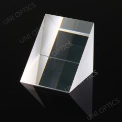 bbar beschichtete Hypotenuse-Winkelprismen
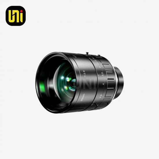
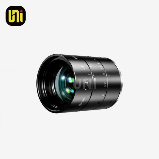
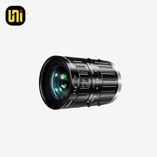
 ITS Lens UN-AT25014SIR-14MP
For Intelligent Transportation Systems (ITS) Applications: Road Surveillance, ANPR/ALPR, Automatic Incident Detection, Traffic Enforcement Systems, Railway/Tunnel Safety Monitoring, etc.
· Excellent edge sharpness and uniform illumination
· Designed to resist strong light interference, adaptable to complex lighting conditions
· High stability and low distortion ensure measurement accuracy
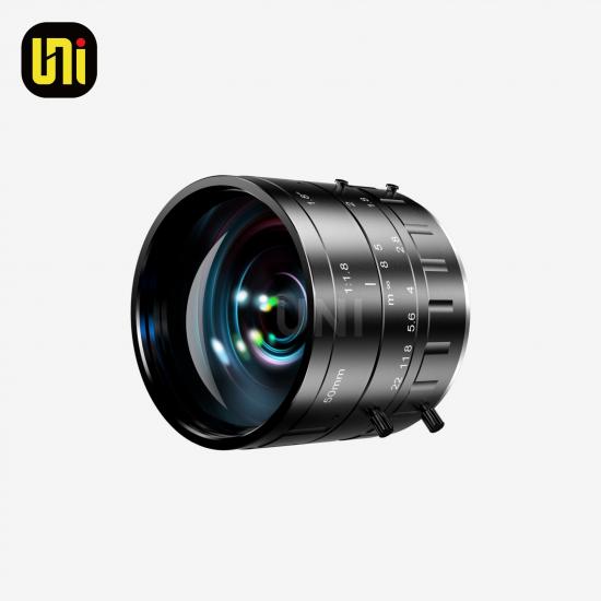
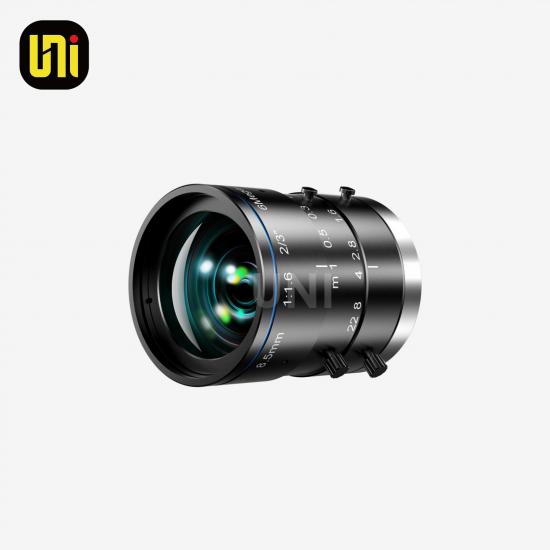
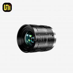 UN-TFA2528L-20MP
· Hohe relative Ausleuchtung und hoher Kontrast
· Geringe Verzerrung und hervorragende Eckenhelligkeit
· Hohe Auflösung
· Kompatibel mit 1''- und 1,1''-20-MP-Kameras
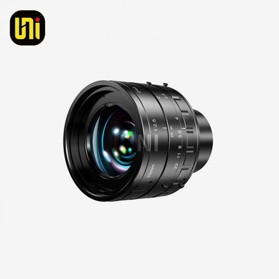
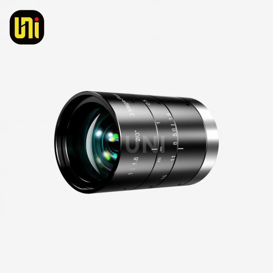
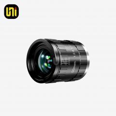 UN-TFA5028L-20MP
· Hohe relative Ausleuchtung und hoher Kontrast
· Geringe Verzerrung und hervorragende Eckenhelligkeit
· Hohe Auflösung
· Kompatibel mit 1''- und 1,1''-20-MP-Kameras
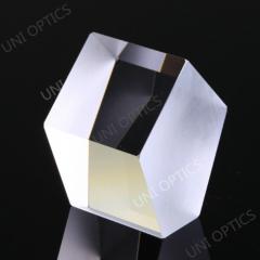 mgf2-beschichteter Pentaprisma-Strahlteiler
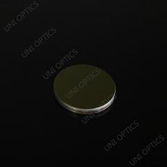 ir windows germanium windows
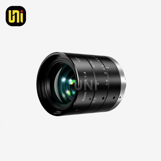
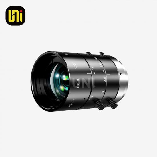
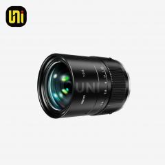 UN-CLS963.5/V45
Produkteigenschaften:
· Abdeckung eines großen Arbeitsabstandsbereichs
· Sehr geringe Verzerrung und hohe Auflösung· Arretierbare Entfernungs- und Blendeneinstellungen
Produktinformationen: Sonderanfertigungen sind auf Anfrage möglich.
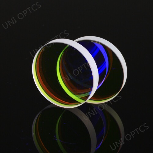
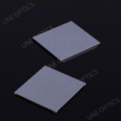
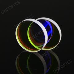 Hochleistungs-Laserlinienfenster
1 、 Was ist Laser Windows?
Laserschutzfenster (Laserschutzglas, Schutzfilter oder Schweißschutzfenster) werden eingesetzt, um die hohen Kosten der Laseroptik zu sparen.
2 、 Wofür werden Laserfenster verwendet?
Diese Fenster werden normalerweise in Laserschneidanwendungen, Laserschweißmaschinen verwendet, um die hochpräzise Beschädigung der Laseroptik durch Materialspritzer zu vermeiden.
3 、 die Hauptmerkmale der Laserfenster von uni optics
hohe übertragung
hohe Schadensschwelle
geringe Streuung
geringe Absorption
ausgezeichnete Filmdichte
ausgezeichnete Umweltstabilität
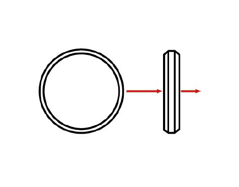
typische spezifikationen:
Abmessung: 4mm-80mm, rund oder quadratisch
material: bk7, quarzglas, znse ... etc.
Oberflächenqualität: 10/5
Oberflächenebenheit: lambda/10@632.8nm
Parallelität: 30 "
Rauheit: 3a
 hochreflektierende breitbandige dichroitische Spiegel
Urheberrechte © © UNI OPTICS CO., LTD © Alle Rechte vorbehalten.
 Tel : +86-591-86395085
 Email : sales@uni-optics.com